The semiconductor industry depends on ultrapure water (UPW) for mission-critical processes like wafer cleaning, rinsing, and CMP. As chip geometries continue to shrink and architectures evolve—think 3D NAND and nanosheet transistors—the margin for error narrows. Even trace-level contaminants in UPW can introduce defects, reduce yields, and compromise device performance. This growing sensitivity exposes serious gaps in current UPW metrology capabilities.
Current Detection Limits Fall Short
Traditional methods struggle to reliably detect particles smaller than 50 nm, yet these so-called "killer" particles—often smaller than that threshold—can disrupt advanced manufacturing steps. Industry goals now target detection down to 10 nm, but existing technologies simply can’t get there. As a result, metrology is often trailing behind process requirements, creating blind spots in contamination control.
Recontamination Risks Post-Filtration
Another challenge lies in material shedding downstream of filtration. High-purity components used after the final filters aren’t always characterized for ultra-fine particle release. That means even well-treated UPW can become recontaminated just before it reaches the wafer, defeating the purpose of upstream purification efforts.
TSI: Leading the Way in Inline Monitoring
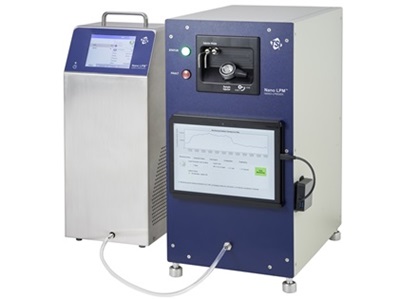
 Monitoring solutions are starting to emerge, and TSI is helping lead that charge. The TSI Nano LPM™ System delivers stable and repeatable in line measurement of UPW water quality, offering a clearer view into a once-invisible risk zone. As more fabs recognize the importance of inline monitoring, the TSI Nano LPM System is poised to play a critical role in closing longstanding metrology gaps.
Learn more about the TSI Nano LPM System >
 汉语
汉语
 English
 Français
 Deutsch


