See What Optical Methods Miss
CMP Slurry Characterization
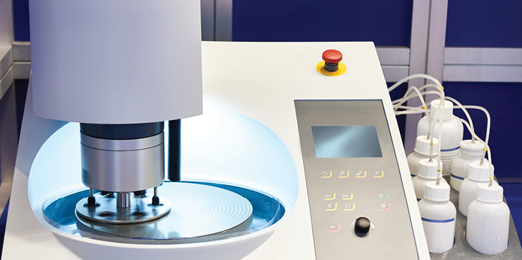
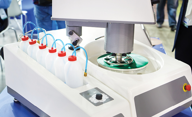
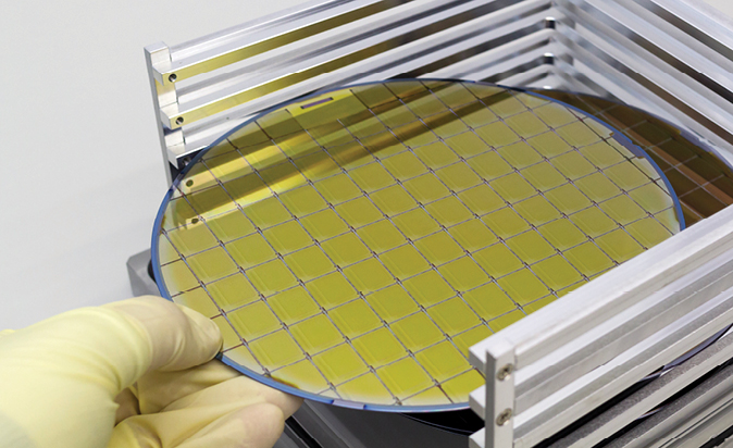
Chemical Mechanical Planarization (CMP) is a critical process in semiconductor manufacturing, using carefully engineered slurries to achieve the ultra-flat, defect-free wafer surfaces demanded by advanced device nodes. These slurries are complex, multicomponent colloidal systems comprising abrasive nanoparticles. dispersed within a liquid chemical matrix of oxidizers, corrosion inhibitors, surfactants, and polymeric additives. The interplay between chemistry and mechanical abrasion governs the material removal process, making precise control of slurry composition essential to yield.
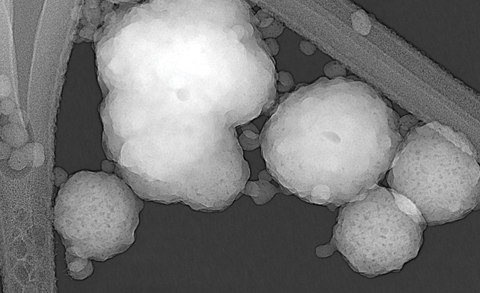
At the heart of that control is the abrasive particle size distribution (PSD): it is a key factor influencing the material removal rate (MRR), within-wafer non-uniformity (WIWNU), surface roughness, and defect density, making it an important parameter in CMP process optimization. Yet the most widely used characterization technique — dynamic light scattering (DLS) — cannot reliably measure sub-30 nm fines, and resolve multimodal distributions, . TSI's Atomizer and Scanning Mobility Particle Sizer (SMPS) system changes that.
 汉语
汉语
 English
 Français
 Deutsch