800-680-1220 / +1 651-490-2860 (US) All Locations

Wafer and Reticle Contamination Standards

Improving your surface defect inspection

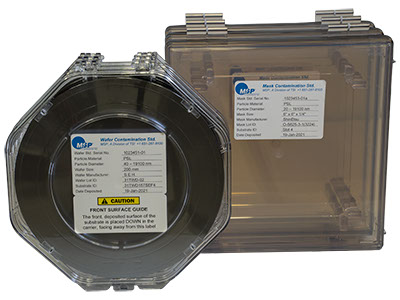
Wafer & Reticle Contamination Standards

Wafer and Photomask Contamination Standards

Programs developed to meet your needs Deposition Services.

High-quality surface defect contamination standards:

  • improve overall performance of your semiconductor manufacturing inspection systems,
  • reduce inconsistencies within your inspection/metrology tool fleet, and
  • maximize device yield

MSP, a Division of TSI, supplies wafer contamination standards and reticle contamination standards in the semiconductor industry for consistent and repeatable particle size and count control.

MSP provides certified standards for wafer and reticle inspection tools for developing, qualifying, calibrating, and monitoring wafer and reticle/photomask inspection systems. Particles of specified size, composition, and count are deposited on your substrate of choice, including wafers, 6-inch reticles (any type), and other less common substrates. Particles can be deposited on bare, film, and patterned wafers from 100mm to 300mm.

Download the Wafer & Photomask Surface Defect Contamination Standards brochure to learn how MSP can help improve your surface defect inspection!


Develop. Deploy. Deliver.

Our wafer and reticle contamination standards are used for the development of semiconductor inspection tools, process tools, and manufacturing processes. They are used in fabs with inspection systems and processes for qualification and acceptance, as well as for maintenance of equipment/processes and performance for the duration of their service lives. MSP’s contamination standards enable high-volume manufacturing (HVM) and delivery of electronic devices.

Dev-Dep Development Contamination StandardsDevelop: MSP Dev-Dep™ Development Contamination Standards

MSP Dev-Dep™ Development Contamination Standards help accelerate product and process development. These standards are totally customized to suit the unique and challenging requirements of your application with support from MSP's particle deposition experts.
 

Qual-Dep Qualification Contamination StandardsDeploy: MSP Qual-Dep™ Qualification Contamination Standards

MSP Qual-Dep™ Qualification Contamination Standards accompany inspection systems installed in semiconductor fabs. These are tool-specific standards which reliably demonstrate in-field performance, reduce risk to acceptance, and help match systems. OEM wafer and reticle contamination standards can be purchased in volume with dedicated part numbers and lower prices.

Cal-Dep Calibration Contamination StandardsDeliver: MSP Cal-Dep™ Calibration Contamination Standards

Inspection systems need to be calibrated regularly throughout their service lives to ensure consistent performance, which is critical for statistical process control (SPC) as part of advanced process control (APC) in device manufacturing. MSP Cal-Dep™ Calibration Contamination Standards are highly accurate standards to help you maintain your tool’s performance, so your manufacturing process can consistently deliver high-quality product. Deposited with well-defined recipes, these wafer/photomask contamination standards can be produced quickly for fast delivery.

Accurate and Traceable. Precise and Repeatable.

Our Differential Mobility Analyzers (DMA) precisely control the mode (peak) of, and variation in, deposited particle diameter. DMAs are calibrated with SI traceability using the best available particle size reference materials, including PSL spheres from NIST.

MSP’s particle size (10 nm to 20 μm) and count (400 to >100,000 particles per deposit) are extremely repeatable from substrate to substrate. Spot diameter (typically 10-30 mm) and spot location are consistent from deposit to deposit (adjustable with sub-millimeter precision).

Our quick substrate processing speed means your contamination standards are returned to you swiftly. The faster the turnaround, the faster your product can be developed, qualified, and calibrated.

MSP’s Wafer and Reticle Contamination Standards meet today’s inspection and metrology applications, including:

  • Traceable calibration and matching legacy calibration standards
  • Incoming bare wafer inspection/qualification
  • Blanket film monitoring
  • Incoming reticle inspection/qualification
  • Production reticle monitoring
  • Inspection tool development and qualification
  • Process tool qualification and monitoring
Page 1 of 1
Items Per Page