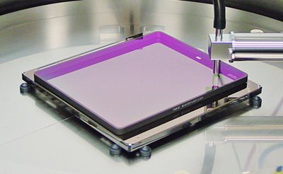
 In the world of semiconductor manufacturing, where precision and innovation go hand in hand, the significance of photomask contamination standards cannot be overstated. These seemingly unassuming standards are essential tools used by leading-edge equipment suppliers, mask shops at prominent device manufacturers, and other key players in the semiconductor industry. They play a crucial role in developing, qualifying, and calibrating defect mask inspection and review systems, ultimately contributing to the production of high-quality semiconductor devices.
Setting the (Photomask Contamination) Standard
Photomask contamination standards are not as widely recognized as other high-tech components in the semiconductor industry, but their role is pivotal in ensuring the quality and reliability of semiconductor devices. These standards are used to qualify inspection and review tools during process development and for periodic quality checks during manufacturing. Essentially, they serve as a benchmark for assessing the integrity of photomasks and pellicles.
 The Making of Photomask Contamination Standards
Creating these standards involves a meticulous process. Contamination standards are produced by depositing soft defects of known composition, size, and morphology at specific locations on a mask or pellicle surface. A typical standard consists of multiple circular spot deposits, each containing hundreds to thousands of uniformly dispersed particles. The remarkable aspect is that the electrophoretic deposition process used to create these standards is virtually indifferent to the substrate, making it applicable to various materials used in the semiconductor industry.
Challenges and Innovations of Contamination Standards
Over the past decade, significant challenges have been met and overcome in the development of photomask contamination standards. These challenges include achieving sub-nanometer repeatability in nanoparticle size, depositing particles on mask edges (bevel and sidewall), depositing large particles up to 20μm in diameter, and ensuring safe deposition on fragile pellicles. The ability to inspect deposits on wafers as a proxy for mask and pellicle inspection has been enabled by repeatable deposition processing.
Particle Material Evolution
The materials used to create photomask contamination standards have evolved over time in response to changing inspection capabilities and challenges. Polystyrene latex (PSL) spheres, which were widely used as size standards for decades, have largely been replaced by silica (SiO2) spheres. SiO2 spheres have proven to be more robust and capable of withstanding intense UV (ultraviolet) energies (Syedain et al, 2013).
Furthermore, recent advancements have allowed for the deposition of different defect materials such as alumina, silicon nitride, tin, and tungsten. This innovation allows these standards to emulate process-induced defects found in the real world, ensuring that inspection and review tools are capable of identifying and addressing issues that can occur during semiconductor manufacturing.
Pivotal Role of Photomask Contamination Standards
In the intricate world of semiconductor manufacturing, precision and reliability are paramount. Photomask contamination standards may not be in the limelight, but they are the unsung heroes that underpin the industry's success. These standards, developed with meticulous care and innovation, play a pivotal role in ensuring the quality, reliability, and manufacturing yield of semiconductor devices by helping mask shops and mask inspection OEMs optimize defect inspection equipment performance and defect reduction processes. As technology continues to advance, the world of photomask contamination standards will evolve as well, contributing to the ongoing progress of the semiconductor industry.
Learn More About our Deposition Calibration Standards - Click Here.
 汉语
汉语
 English
 Français
 Deutsch


