 汉语
汉语
 English
 Français
 Deutsch


Even the tiniest particle left behind during the cleaning process can lead to significant defects and costly yield issues. If a wafer is not cleaned sufficiently and particles are unknowingly left behind during a given processing step, those particles may create killer defects later in the device manufacturing process. Our consistent, uniform and fundamentally minimally aging dryly deposited PRE standards assist in validating and optimizing the cleaning system and process, alerting users that the tool needs attention. Contaminated wafers and masks impact fab productivity and profitability due to lost time and lower yield.
Contamination Particle Selection
MSP's PRE Challenge Wafers and Photomasks for Particle Removal Efficiency (PRE) can be deposited using NanoSilica™ Size Standards, Polystyrene Latex (PSL) or Process Particles™. The flexibility in using these different particles serve drastically different applications and provide different benefits when used to evaluate a cleaning system or process.Nanosilica™ and PSLs
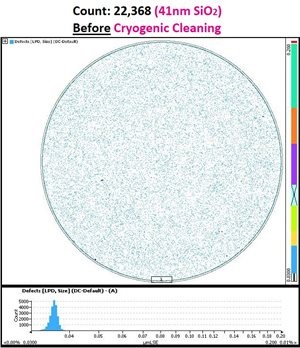
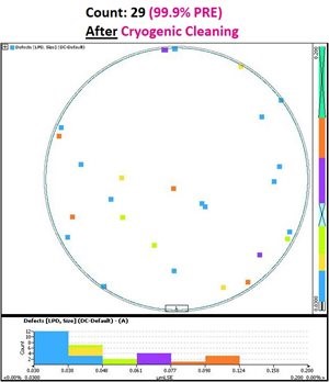
MSP’s NanoSilica™ and PSL standards are concentrated suspensions of amorphous SiO2 and PSL particles with highly uniform size distributions in ultra-pure water (UPW). Deposition of a single particle size allows the evaluation of PRE spatial dependence without interference from other particle sizes.Displayed below is an example of two PRE Challenge Wafers deposited with our narrow distribution NanoSilica particles (41nm peak diameter). It demonstrates the resultant particle size and spatial distributions from wafer inspection and particle distribution prior to and after undergoing a cryogenic cleaning process.
Process Particles™ Suspensions
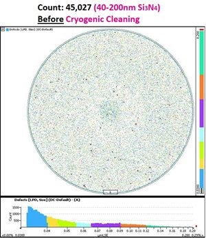
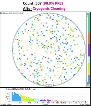
MSP's Process Particles™ Suspensions consist of broad size distributions of irregularly shaped solid particles suspended in ultra-pure water (UPW). They represent real-world contaminant particles encountered in semiconductor device fabrication processing. Process Particles Suspensions have wide distributions of particle sizes, which more accurately simulate the contaminant particles present on a wafer or photomask in a real-world scenario, allowing size-dependent PRE to be evaluated more efficiently. Process particle distributions can also be narrowly distributed to optimize a process for a given concerning size.Displayed below is an example of two PRE Challenge Wafers deposited with our Process Particles Suspensions. The images below show the particle size and spatial distributions from wafer inspection prior to and after undergoing a cryogenic cleaning process.
Learn More About Surface Defect Inspection and More Solutions We Provide - Click Here.