 The Significance of Particle Deposition
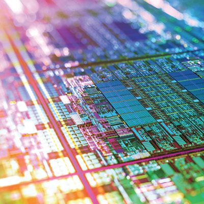
In semiconductor manufacturing, the identification and classification of defects as small as 10nm are essential for maintaining high yields and quality. However, detecting such tiny defects poses significant challenges. To overcome these challenges, advanced inspection systems are required, and this is where particle deposition comes into play.
Understanding the Particle Deposition System
The Particle Deposition System (PDS) 2300G3 is a cutting-edge tool designed for the precise deposition of particles with known characteristics, including size, morphology, and optical properties. One of the primary applications of PDS is the calibration of wafer and photomask defect inspection systems. These systems rely on the intensity of light scattered by defects when illuminated by an intense laser to detect and characterize those defects.
The PDS operates in two modes: DMA mode and Direct mode. In DMA mode, a Differential Mobility Analyzer (DMA) is used to select a narrow range of particles from a particle suspension, providing high accuracy in particle size control. The system generates aerosolized particles by atomizing a dilute suspension in ultrapure water, and these particles are then classified based on electrical mobility in the DMA.
Challenges and Achievements in Particle Deposition
One of the most significant achievements attained with MSP’s 2300G3 PDS is the successful deposition of 10nm silica nanoparticles with precise control of particle size, deposit location, and areal number density. This achievement has been validated using advanced microscopy techniques, including Atomic Force Microscope (AFM) and Scanning Electron Microscope (SEM).
Insights from TEM Grid Deposition Attempts
Initial attempts to deposit silica particles on TEM grids, which are used for transmission electron microscopy, were unsuccessful. While challenges related to particle deposition and grid arcing were encountered, they shed light on the complexities of particle deposition at the nanoscale.
Deposition and Analysis on Silicon Wafers
Successful 10nm silica particle deposition was achieved on silicon wafers, followed by analysis using SEM and AFM. These analyses confirmed the precision of particle deposition, with particle sizes and areal number densities closely matching predictions.
Producing Devices with High Yield
In the ever-advancing semiconductor industry, precision is paramount. Successful validation of the ability of MSP’s PDS to deposit 10nm particles with predictable control of modal diameter and areal number density paves the way for the continued development of advanced defect inspection systems, ultimately contributing to the production of cutting-edge, high-performance semiconductor devices with high yield.
Learn More About Surface Defect Inspection
Or contact the experts via the form if you have specific questions.
 Français
 汉语
汉语
 English
 Français
 Deutsch

