 Support your semiconductor inspection tool throughout its lifecycle
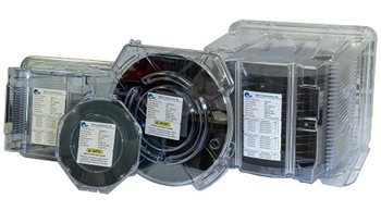
MSP, a Division of TSI, is proud to introduce three new categories of wafer and reticle/photomask contamination standards, which will help you test your inspection/metrology systems.
MSP Dev-Dep™ Development Contamination Standards
- Wafers and photomasks/reticles that are totally customized to suit your application’s unique and challenging requirements (with the support of MSP’s particle deposition experts). These standards help to accelerate product and process development.
MSP Qual-Dep™ Qualification Contamination Standards
- Wafers and photomasks/reticles that accompany inspection systems installed in semiconductor fabs. These are tool-specific standards that reliably demonstrate in-field performance, reduce risk to acceptance, and help match systems.
MSP Cal-Dep™ Calibration Contamination Standards
- Wafers that help you maintain your inspection tool’s performance so your manufacturing process can consistently deliver high-quality product. Inspection systems need to be calibrated regularly throughout their service lives to ensure consistent performance. MSP Cal-Dep™ Calibration Contamination Standards are specially designed for individual inspection tools (specifically SP1 and SP2) and can be delivered with short lead times to help you test your tool and ensure it is performing within your specifications.
Learn more about these new products, and request a quote today!
 English
 汉语
汉语
 English
 Français
 Deutsch

