 汉语
汉语
 English
 Français
 Deutsch


Versatile Water-Based Condensation Particle Counter 3789
Wasserbasierte Partikelzähler (Water-Based Condensation Particle Counters, kurz WCPCs) liefern präzise gemessene Konzentrationen gasgetragener Partikel unter Verwendung von umweltfreundlichem, sicherem und überall verfügbarem destilliertem Wasser. In Verbindung mit einem...

Semiconductor Manufacturing with Glass Wafers
Glass wafers are increasingly used in semiconductor manufacturing. Learn more about the benefits and how MSP can help enhancing inspection systems with precise calibration and contamination standards.

Filling the Ultrapure Water Monitoring Gap
As semiconductor processes become more sensitive, emerging UPW monitoring solutions are closing critical detection gaps by enabling real-time, nanoscale particle measurement that traditional methods miss.
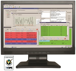
AeroTrak-Plus Remote Particle Counter with Integrated Pump 6000 Series
Durchfluss 2,83 LPM (0,1 CFM) / Kanalgrößenoptionen 0,2 bis 25 μm / Integrierte Pumpe

Meeting ISO 14644 Standards in Cleanrooms
Compliance with ISO 14644 standards is essential to control airborne particulate contamination levels.

Meet Tomorrow's Challenges with Nanoscale Expertise — Tools Essential for Ensuring Precision, Quality Control, and Reliability
We offer cutting-edge solutions tailored to the unique (nanoscale) challenges of the semiconductor manufacturing market. With our advanced instrumentation and expertise, we provide critical tools for process control, quality assurance, and cleanroom monitoring.
Stay ahead of...

Advancing Semiconductor Inspection Tools With Precision
Discover how MSP's Particle Deposition System enables precise calibration of defect inspection systems crucial for maintaining high yields and quality in sub-10nm semiconductor devices.


Drive Consumer Electronics Advancement Through High-Quality Components
Component and consumer electronics involve the assembly of various sophisticated devices like smartphones, tablets, wearables, TVs, and other sensitive optical and electronic products. The manufacturing of these products often occurs in cleanrooms to produce components like...
93 results found