 English
 汉语
汉语
 English
 Français
 Deutsch



产品详情
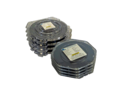
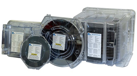
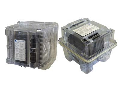
SP3, SP5, and SP7 Wafer Calibration Standards are precision-engineered tools for the calibration, verification and re-qualification of the most common wafer surface inspection systems (like Surfscan® from KLA) used in semiconductor manufacturing. These standards play a crucial role in ensuring the accuracy and reliability of inspection equipment, which is essential to maintain high yields and quality in mature nodes of semiconductor fabrication for years to come.
Based on a combination of industry-leading equipment knowledge and particle deposition expertise, MSP provides a comprehensive line of NIST-traceable Calibration Standards, including documentation of manufacturing processes and controls, inspection reports using a Surfscan® tool, and other certification guarantees. This helps ensure that customers receive best-in-class standards with the narrowest particle distributions, highest particle size accuracy for their critical surface inspection applications.
MSP's Cal-Dep™ portfolio ensures that this industry workhorse inspection equipment is calibrated to factory standards so fabs can continue to operate at peak performance.
Our Offering - Request a quote to see all variants!
SP3 — Full-Wafer, Single Size Only
Broadest range of simple single-size wafers.- 14 nominal/NIST sizes, 32nm–1500nm
- Count: 20,000 ± 6,000
SP5 — Full-Wafer + Multi-Spot Options
Adds multi-spot flexibility.- Full deposit (3 nominal/NIST sizes: 60/90/300nm) — count 20,000 ± 6,000
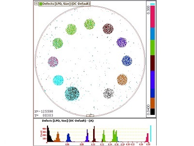
- Multi-spot (dual/6-spot/8-spot, covering 22nm–1500nm) — count 2,000 ± 600
SP7 — Full-Wafer + Multi-Spot + Finest Sizes
Adds the finest particle sizes (down to 18nm) and a unique combo full+center-spot design.- Full deposit (60nm) — count 20,000 ± 6,000
- Full + center-spot combo (60nm) — dual count spec
- Multi-spot (dual/6-spot/8-spot, covering 18nm–1500nm) — count 2,000 ± 600
Applications
- Inspection tool qualification
- Inspection tool calibration
- Process tool monitoring
- Bare silicon wafer IQC/OQC
- Advanced Process Control (APC)
Features and Benefits
- NIST-traceable particle sizing
- Using SiO2 particle depositions
- Full range of wafer configurations (single-size to 8-spot)
- Industry-leading calibration accuracy
- Broad particle size coverage (18nm–1500nm)
- Built for fab-floor use
- Fast delivery
- Simple, streamlined ordering
- OEM-compliant calibration
- Particle sizes matched to original calibration curves
Surfscan is a registered trademark of KLA Corporation.
 英语(英国)
 英语(美国)