 汉语
汉语
 English
 Français
 Deutsch


Direct Answer: The MSP Recertification Program extends the operational life of calibration wafers and optimizes budgets with NIST-traceable recertification. This service helps verify that particle and contamination standards are performing to specifications, ensuring the continued accuracy of wafer inspection systems. By restoring existing wafers to their required performance levels, you achieve significant cost-saving benefits compared to purchasing new replacements all the time. Recertification provides a reliable, compliant, and cost-effective solution for maintaining the precision of critical semiconductor metrology and inspection tools.
Table of Contents
Is Your Calibration Wafer Still Meeting Specifications?
Calibration and monitoring wafers are critical investments in your quality program. But over time, uncertainty grows:
- Particle count drift: Are your deposited particles maintaining their original density, count and distribution?
- Contamination concerns: Has your wafer accumulated fall-on particles that skew results?
- Size variation: Are laser exposure or environmental factors causing particle size drift?
- Compliance gaps: Does your wafer still meet your quality program's traceability requirements?
Replacing calibration wafers is expensive. Continuing to use wafers with unknown performance introduces risk.
MSP's Wafer Recertification Program delivers certainty.
NIST-Traceable Verification for Critical Calibration Standards
Our recertification service provides complete verification of your contamination wafers using the same precision equipment and NIST-traceable processes used to manufacture new standards.
 Program Specifications
Supported Substrates
- 200mm and 300mm bare silicon wafers
- SiO2 and PSL particle materials
- Size range: 37nm to 6,000nm
Inspection Process
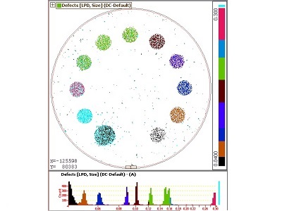
- KLA Surfscan® inspection system
- Custom recipe development for your specifications
- Exclusion zones and custom parameters supported
- Class 100 cleanroom handling throughout
Documentation Package
- NIST-certified size certificate
- Complete SSIS inspection report
- Original wafers returned in triple-pack cleanroom packaging
- Full traceability documentation
Turnaround Time
- Standard 4-week lead time from receipt
How It Works
1. Submit Your Wafer Information
Complete our order questionnaire with wafer specifications, orientation markers, calibration locations, and particle materials. We'll confirm receipt and provide shipping instructions.
2. Ship Your Wafers
Package your wafers following our cleanroom-compatible guidelines. We provide detailed packaging recommendations to ensure contamination-free transport.
3. Inspection and Certification
Our team develops custom Surfscan® recipes matching your original specifications, inspects your wafers in our Class 100 cleanroom, and generates comprehensive certification documentation.
4. Receive Verified Standards
Your recertified wafers return with complete documentation packages in cleanroom-compatible packaging, ready for immediate use in your fab environment.
Why Choose MSP for Wafer Recertification?
Proven Expertise: MSP's Semiconductor Metrology Group has delivered contamination standards to leading semiconductor manufacturers for decades.
NIST Traceability: Our inspection equipment and processes provide the same NIST-traceable verification used for new calibration wafer manufacturing.
Cost Efficiency: Verify wafer performance at a fraction of new wafer replacement costs while maintaining full traceability. Extending the guaranteed useful life of the standard.
Cleanroom Standards: Class 100 cleanroom handling throughout the entire process ensures no additional contamination.
Frequently Asked Questions
What wafer types can be recertified?
We support 200mm and 300mm bare silicon wafers with SiO2 or PSL particle depositions. Particle sizes from 37nm to 6,000nm can be verified. Both spot deposits and full calibration sets are supported.
How does recertification compare to purchasing new wafers?
Recertification provides NIST-traceable verification using the same equipment and processes as new wafer manufacturing, at significantly reduced cost. If your wafer meets specifications, recertification extends its usable lifetime while maintaining full traceability.
What documentation do I receive?
Each recertified wafer includes a NIST-certified size certificate, complete SSIS inspection documentation package, and the original wafer returned in triple-pack cleanroom packaging.
What is the standard turnaround time?
Standard lead time is four weeks from wafer receipt. Contact us for expedited service options.
How should I package wafers for shipping?
We recommend triple-layer packaging: heat-sealed nylon-poly bag, second protective layer, and outer foil moisture barrier. Include desiccant and ship in a padded box. Complete guidelines are provided with your service order.
What if my wafer doesn't meet specifications?
If inspection reveals contamination, excessive particle drift, or other issues that prevent certification, we provide detailed findings You can decide whether to proceed with the standard as is or if it is time for a replacement.
Can you accommodate custom inspection requirements?
Yes. We develop custom KLA Surfscan® recipes to match your specific requirements including exclusion zones, detection thresholds, and custom parameters.
Maintain Quality Program Compliance with Verified Calibration Standards
Stop questioning whether your calibration wafers are performing to specification. MSP's Wafer Recertification Program delivers NIST-traceable verification that extends wafer lifecycle while reducing total cost of ownership.
More About the MSP Recertification Program
*Surfscan is a registered trademark of KLA Corporation.